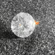
Researchers in France, Britain and Japan have improved the channel mobility performance of diamond MOSFETs by doping with boron
Diamond materials · Power electronics
How Deep Depletion Could Improve Diamond MOSFET Channel Mobility
A 2017 proof-of-concept study explored a different way to operate a boron-doped diamond MOSFET. Its deep-depletion approach aimed to retain a high-mobility bulk hole channel while switching the device off through a depleted region beneath the gate.
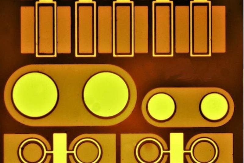
Research context: The work described here was published in 2017 as a proof of concept. It does not establish that diamond MOSFETs are widely manufactured or commercially available for mainstream power electronics.
Why investigate diamond transistors?
A metal-oxide-semiconductor field-effect transistor (MOSFET) uses an electric field from a gate to control current in a semiconductor channel. Diamond is being studied for power electronics because its material properties are attractive for devices intended to operate under demanding electrical and thermal conditions.
Material properties alone do not make a practical transistor. Researchers must also control the channel, gate dielectric, interfaces, contacts and manufacturing process. In diamond MOSFETs, achieving useful channel mobility while maintaining reliable gate control has been an important research challenge.
What the deep-depletion concept changes
The international team studied a device built on a boron-doped diamond epitaxial layer. Boron makes the diamond p-type, with positively charged holes serving as the mobile carriers in the conducting channel.
On state
With the channel conducting, current flows through the boron-doped diamond layer between the source and drain.
Off state
Applying a gate voltage depletes mobile holes beneath the gate. In the reported device, this deep-depletion region acts as an insulating region and interrupts the channel.
The researchers used an aluminium oxide (Al₂O₃) gate-insulator layer on oxygen-terminated diamond. Their reported approach was designed to reduce reliance on a surface channel at the oxide–diamond interface, where roughness and defects can scatter carriers and affect measured mobility.
What “higher mobility” means in this study
Carrier mobility describes how readily charge carriers move through a material when an electric field is applied. In a transistor, mobility is one factor that influences how much current the channel can carry; it is not, by itself, a complete measure of device performance.
The original research coverage reported an approximately order-of- magnitude mobility increase for the deep-depletion concept compared with the approaches discussed in that report. This is a result tied to the study’s device structure and comparison. It should not be read as a universal improvement for every boron-doped diamond device or as a commercial product specification.
What the result does—and does not—show
A device concept was demonstrated
The paper reported a proof of concept for using deep depletion in a boron-doped diamond MOSFET structure.
It is not a production announcement
A laboratory result does not by itself prove scalable manufacturing, long-term reliability, cost competitiveness or broad market adoption.
More engineering remains
Device consistency, interfaces, contacts, wafer growth, packaging and qualification all matter when moving from a research device toward practical applications.
Why it matters for diamond research
The study offered a route for investigating how diamond’s wide bandgap could support a stable deep-depletion operating regime. It also helped focus attention on the relationship between the conducting bulk channel and the gate-controlled depleted region.
Diamond electronics remain an active research area. Potential uses in demanding power or high-temperature environments depend on further device development and validation; the 2017 result alone does not establish readiness for those applications.