Could CVD Diamond Help Cool Future Processors
Diamond Materials · Electronics
CVD Synthetic Diamond: Could It Help Cool Future CPUs?
Chemical vapour deposition (CVD) can produce synthetic diamond films and crystals for industrial applications. Engineers are studying diamond as a heat-spreading material for demanding electronic devices, including some semiconductor and processor packaging designs.
A heat spreader is not a “diamond processor”
CVD diamond may help move heat away from a semiconductor. That is different from replacing the silicon logic in a CPU with diamond. Large-scale use in consumer processors remains a possibility to investigate, not an established outcome.
What is CVD synthetic diamond?
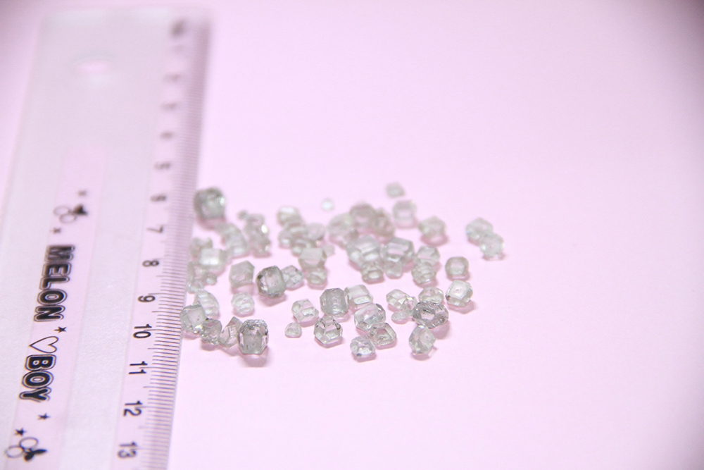
CVD is a process for growing diamond from carbon-containing gases in a controlled environment. A carbon source, often used with hydrogen, is activated by heat or plasma. Carbon species then deposit on a prepared surface and form diamond under suitable growth conditions.
Common approaches include hot-filament CVD and microwave-plasma CVD. Depending on the process, seed material and growth conditions, CVD can produce polycrystalline films or single-crystal material. The method describes how the diamond is made; it does not by itself specify the material’s quality or intended application.
CVD-grown diamond is diamond, but industrial material is engineered for its particular use. It is not automatically equivalent to a natural jewellery diamond in appearance, grading or market value.
Properties depend on the material
High-quality diamond can conduct heat very effectively. Some high-quality material has a room-temperature thermal conductivity above 2,000 W/(m·K), but this should not be treated as a value for every CVD film or diamond component.
Thermal performance varies with crystal form, grain size, defects, impurities, thickness, processing and measurement conditions. Interfaces between diamond and other device materials can also limit how much heat is transferred out of a chip.
Polycrystalline diamond
Made up of many crystal grains. Grain boundaries and defects influence the finished material’s thermal and mechanical properties.
Single-crystal diamond
Has one continuous crystal orientation across the material. Growth, size, defects and processing remain important to the performance of a particular component.
Why use diamond for heat management?
As power density increases, heat can become concentrated in small regions of a semiconductor. A heat spreader is designed to move energy away from these hot spots and toward the rest of the cooling system.
Diamond’s high thermal conductivity makes it a candidate for this role in selected high-power or high-frequency devices. The diamond layer is one part of a thermal path that may also include the semiconductor, bonding or interlayer materials, package, heat sink and cooling system.
Applications beyond CPU cooling
Cutting tools and wear surfaces
CVD diamond coatings and films can be used in tool applications where hardness and wear resistance are useful. Tool design, adhesion and operating conditions affect performance.
Thermal management
Diamond materials are studied for heat spreaders, substrates and packaging in electronics that generate concentrated heat.
Optical windows
Selected CVD diamond materials can transmit light across broad wavelength ranges, making them useful candidates for windows in demanding optical environments.
Detectors and sensing research
Diamond’s radiation tolerance and engineered defects are studied for specialist detectors and quantum-sensing research. These applications depend on carefully controlled material properties.
Could CVD diamond be used in future CPUs?
It is more accurate to ask whether diamond can help cool selected processor or semiconductor packages than to ask whether CPUs will be made from diamond. Research has examined diamond structures in advanced chip packaging and thermal-management designs, but a demonstration in a test structure does not establish routine adoption in mass-market processors.
Undoped diamond is electrically insulating. Doping can change its electrical behaviour, but diamond electronics face separate material and manufacturing challenges. A diamond heat spreader therefore should not be confused with a diamond logic chip.
What still needs to be solved?
- Interface resistance: heat may encounter resistance where diamond meets silicon, gallium nitride, bonding layers or other package materials.
- Growth and integration: the process must create the required diamond layer without damaging temperature-sensitive device structures.
- Material consistency: defects, grain boundaries, thickness and surface quality affect component performance.
- Processing: diamond’s hardness and chemical stability make cutting, polishing, bonding and other finishing operations demanding.
- Manufacturing economics: high-quality material and compatible production steps must be available at a cost and scale that make sense for the target device.
A promising material, with application-specific limits
CVD diamond combines useful thermal, mechanical, optical and electrical characteristics. Different applications require different combinations of those properties, so a material suitable for a cutting tool may not be suitable for an optical window or a semiconductor package.
For processor cooling, the key evidence will be device-level results: reliable integration, improved heat transfer under comparable conditions, manufacturability and a clear benefit over existing package materials.
This article is a general overview of CVD diamond materials and research. Material properties vary with growth and processing. Research demonstrations do not guarantee commercial availability or widespread use in consumer processors.